New Product Launch–Do you know GOB LED display?
1. GOB process
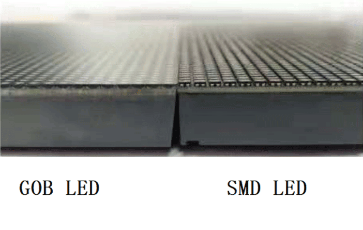
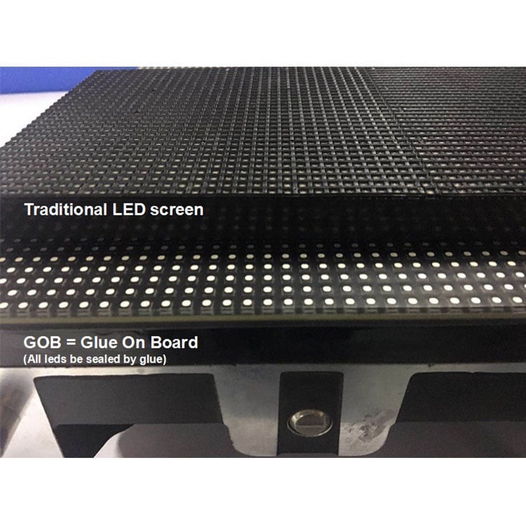
GOB is the abbreviation of GLUE ON BOARD, GOB process is a new optical and thermal conductive nano-fill material, through a special process to the conventional LED display PCB board and its SMD LED lamp for encapsulation and matte dual surface optical treatment, to achieve the matte effect of the LED display surface, enhance the existing LED display protection technology, and GOB is not a breakthrough in packaging technology, but a technological improvement to the existing SMD technology, which essentially still belongs to the SMD technology.

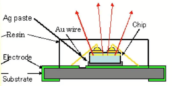
Note: SMD is the abbreviation of Surface Mounted Device, meaning surface mount device, which is a light cup, bracket, chip, lead, epoxy resin and other materials packaged into different specifications of the lamp beads, and then through the form of SMD welding on the PCB board to form the LED display module. It will also make the protection performance poorer and affect the imaging effect and service life.
Moreover, due to the structure of the lamp cups and brackets, there is a physical limit to the size of the pixel of SMD displays. Take the SMD P1.25 LED display as an example, the pixel size can only be as small as 1mm*1mm, and the contrast ratio is generally 3000:1, which is difficult to meet the future development of industry demand for ultra-high definition display.

2. GOB LED Display advantages
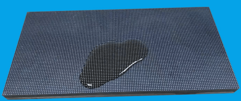
waterproof, moisture, bump, dust, corrosion, blue light, salt-spray, anti-static.

Due to the surface matte effect also increases the color contrast, to achieve the transformation from the display point light source into surface light source display, increasing the viewing angle.
3. GOB LED display disadvantage
(1) GOB packaging materials must be developed with the GOB process program of customized materials, must meet the following characteristics:
1, strong adhesion;
2, strong resistance to tension and vertical impact;
3, hardness;
4, high transparency;
5, temperature resistance;
6, yellowing resistance;
7, salt spray resistance;
8, high abrasion resistance;
9, anti-static;
10, anti-voltage, etc.
(2) GOB packaging process to ensure that the packaging material completely fill the gap and cover the surface of the LED lamp, and PCB closely bonded, there can be no bubbles, air holes, PCB and glue bonding surface white spots, cavities, not filled with the phenomenon.
(3) The consistency of the thickness of the glue layer (accurately described as the consistency of the thickness of the glue layer above the surface of the lamp bead) After GOB packaging, it is necessary to ensure the uniform consistency of the thickness of the glue layer above the surface of the lamp bead. At present, GOB process has been fully upgraded to 4.0, almost no more rubber layer thickness tolerance, the original module thickness tolerance is how much is done after the original module thickness tolerance can even be reduced. Splicing flatness is quite perfect! Adhesive layer thickness consistency for the GOB process is critical, cannot guarantee the modularity of the black screen and lit state, splicing screen, uneven splicing height, poor color consistency and a series of fatal problems.
(4) GOB package after the repairability, to ensure that the package material is easy to take off under certain conditions, after the repair of the glue to take off part of the ability to fill the repair.
At present, GOB LED display technology is mainly used in small pixel pitch products, and its process requires high packaging materials such as “glue”. Generally, new materials such as epoxy resin can be used, and techniques such as inkjet blackening can also be used to enhance screen contrast. Although GOB technology combines many advantages of SMD and COB, it should also be noted that it still has its limitations in terms of advanced technology, and the future application development path will continue to expand with the development of technology and materials.
If you are interested in GOB products, please contact us, we will customize the products you want based on your needs.
Get In touch
(86) 186-76693660
available from 9:00 – 18:00
Address :NO.19 LongGang Road ShenZhen
Email :info@jindaxiang.cn
